|
|
|
PDF AD8027 Data sheet ( Hoja de datos )
| Número de pieza | AD8027 | |
| Descripción | Rail-to-Rail Input/Output Amplifiers | |
| Fabricantes | Analog Devices | |
| Logotipo | ||
Hay una vista previa y un enlace de descarga de AD8027 (archivo pdf) en la parte inferior de esta página. Total 27 Páginas | ||
|
No Preview Available !
Data Sheet
Low Distortion, High Speed
Rail-to-Rail Input/Output Amplifiers
AD8027/AD8028
FEATURES
High speed
190 MHz, −3 dB bandwidth (G = +1)
100 V/µs slew rate
Low distortion
120 dBc at 1 MHz SFDR
80 dBc at 5 MHz SFDR
Selectable input crossover threshold
Low noise
4.3 nV/√Hz
1.6 pA/√Hz
Low offset voltage: 900 µV maximum
Low power: 6.5 mA per amplifier supply current
Power-down mode
No phase reversal: VIN > |VS| + 200 mV
Wide supply range: 2.7 V to 12 V
Small packaging: 8-lead SOIC, 6-lead SOT-23, 10-lead MSOP
Qualified for automotive applications (AD8028WARMZ-R7 only)
APPLICATIONS
Filters
ADC drivers
Level shifting
Buffering
Professional video
Low voltage instrumentation
GENERAL DESCRIPTION
The AD8027/AD80281 are high speed amplifiers with rail-to-rail
input and output that operate on low supply voltages and are
optimized for high performance and a wide dynamic signal range.
The AD8027/AD8028 have low noise (4.3 nV/√Hz, 1.6 pA/√Hz)
and low distortion (120 dBc at 1 MHz). In applications that use a
fraction of or use the entire input dynamic range and require
low distortion, the AD8027/AD8028 are ideal choices.
Many rail-to-rail input amplifiers have an input stage that switches
from one differential pair to another as the input signal crosses
a threshold voltage, which causes distortion. The AD8027/AD8028
have a unique feature that allows the user to select the input
crossover threshold voltage through the DISABLE/SELECT pin
(DISABLE/SELECT x in the 10-lead MSOP, hereafter referred
to as DISABLE/SELECT throughout this data sheet). This feature
controls the voltage at which the complementary transistor
input pairs switch. The AD8027/AD8028 also have intrinsically
low crossover distortion.
1 Protected by U.S. patent numbers 6,486,737B1; 6,518,842B1.
Rev. D
Document Feedback
Information furnished by Analog Devices is believed to be accurate and reliable. However, no
responsibilityisassumedbyAnalogDevices for itsuse,nor foranyinfringementsofpatentsor other
rights of third parties that may result from its use. Specifications subject to change without notice. No
license is granted by implication or otherwise under any patent or patent rights of Analog Devices.
Trademarksandregisteredtrademarksarethepropertyoftheirrespectiveowners.
PIN CONNECTION DIAGRAM
DNC 1
–IN 2
+IN 3
–VS 4
AD8027
8 DISABLE/SELECT
7 +VS
6 VOUT
5 DNC
DNC = DO NOT CONNECT. DO NOT
CONNECT TO THIS PIN.
Figure 1. 8-Lead SOIC, AD8027
See the Pin Configurations and Function Descriptions section
for additional pin configurations and information about the pin
functions.
With their wide supply voltage range (2.7 V to 12 V) and wide
bandwidth (190 MHz), the AD8027/AD8028 amplifiers are
designed to work in a variety of applications where speed and
performance are needed on low supply voltages. The high per-
formance of the AD8027/AD8028 is achieved with a quiescent
current of only 6.5 mA (typical) per amplifier. The AD8027/
AD8028 have a shutdown mode that is controlled via
the DISABLE/SELECT pin.
The AD8027/AD8028 are available in 8-lead SOIC, 6-lead SOT-23,
and 10-lead MSOP packages. The AD8028WARMZ-R7 is an
automotive grade version, qualified for automotive applications.
See the Automotive Products section for more details. The
AD8027/AD8028 family is designed to work over the extended
temperature range of −40°C to +125°C.
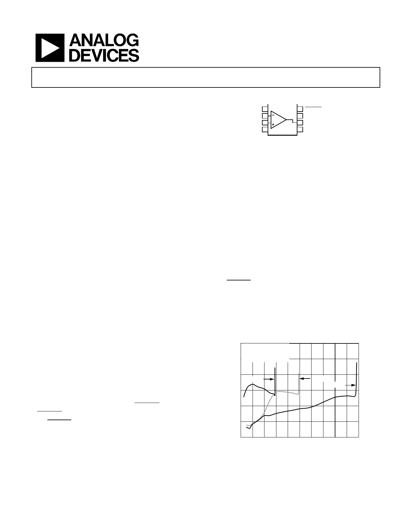
–20
G = +1
FREQUENCY = 100kHz
–40 RL = 1kΩ
–60
VS = +3V
–80
VS = +5V
VS = ±5V
–100
–120
–140
0
12345678
OUTPUT VOLTAGE (V p-p)
Figure 2. SFDR vs. Output Voltage
9 10
One Technology Way, P.O. Box 9106, Norwood, MA 02062-9106, U.S.A.
Tel: 781.329.4700 ©2003–2015 Analog Devices, Inc. All rights reserved.
Technical Support
www.analog.com
1 page 
Data Sheet
AD8027/AD8028
Parameter
INPUT CHARACTERISTICS
Input Impedance
Input Capacitance
Input Common-Mode Voltage Range
Common-Mode Rejection Ratio
DISABLE/SELECT PIN
Selection Input Voltage
Crossover Low
Crossover High2
Disable Input Voltage
Disable Switching Speed
Enable Switching Speed
OUTPUT CHARACTERISTICS
Overdrive Recovery Time
(Rising/Falling Edge)
Output Voltage Swing
Off Isolation
Short-Circuit Current
Capacitive Load Drive
POWER SUPPLY
Operating Range
Quiescent Current per Amplifier
Quiescent Current (Disabled)
Power Supply Rejection Ratio
Test Conditions/Comments
VCM = 0 V to 2.5 V
AD8028W only: TMIN to TMAX
TMIN to TMAX
Tristate < ±20 µA, TMIN to TMAX
TMIN to TMAX
50% of input to <10% of final VOUT
VIN = −6 V to +1 V, G = −1
AD8028W only: TMIN to TMAX
VIN = 0.2 V p-p, f = 1 MHz, DISABLE/SELECT = low
Sinking and sourcing
30% overshoot
AD8028W only: TMIN to TMAX
DISABLE/SELECT = low
AD8028W only: TMIN to TMAX
VS ± 1 V, AD8028W only: TMIN to TMAX
1 No sign or a plus sign indicates current into the pin; a minus sign indicates current out of the pin.
2 It is recommended to float the DISABLE/SELECT pin for crossover high mode.
Min Typ
Max Unit
6 MΩ
2 pF
−0.2 to +5.2
V
90 105
dB
84 dB
2.0 V
1.1 to 1.3
V
0.4 V
1100
ns
50 ns
50/50
0.08 to 4.92
0.04 to 4.96
−49
105
20
ns
V
dB
mA
pF
2.7 12 V
6 8.5 mA
9 mA
320 450 µA
450 µA
90 105
dB
VS = 3 V at TA = 25°C, RL = 1 kΩ to midsupply, G = +1, unless otherwise noted.
Table 3.
Parameter
DYNAMIC PERFORMANCE
−3 dB Bandwidth
Bandwidth for 0.1 dB Flatness
Slew Rate
Settling Time to 0.1%
NOISE/DISTORTION PERFORMANCE
Spurious-Free Dynamic Range (SFDR)
Input Voltage Noise
Input Current Noise
Differential Gain Error
Differential Phase Error
Crosstalk, Output to Output
Test Conditions/Comments
G = +1, VOUT = 0.2 V p-p
AD8028W only: TMIN to TMAX
G = +1, VOUT = 2 V p-p
AD8028W only: TMIN to TMAX
G = +2, VOUT = 0.2 V p-p
G = +1, VOUT = 2 V step
G = −1, VOUT = 2 V step
G = +2, VOUT = 2 V step
fC = 1 MHz, VOUT = 2 V p-p, RF = 24.9 Ω
fC = 5 MHz, VOUT = 2 V p-p, RF = 24.9 Ω
f = 100 kHz
f = 100 kHz
NTSC, G = +2, RL = 150 Ω
NTSC, G = +2, RL = 150 Ω
G = +1, RL = 100 Ω, VOUT = 2 V p-p, VS = 3 V at
1 MHz
Min
125
125
19
19
Typ
180
29
10
73
100
48
85
64
4.3
1.6
0.15
0.20
−89
Max Unit
MHz
MHz
MHz
MHz
MHz
V/µs
V/µs
ns
dBc
dBc
nV/√Hz
pA/√Hz
%
Degrees
dB
Rev. D | Page 5 of 27
5 Page 
Data Sheet
4
G = +1
3 VOUT = 200mV p-p
2
CL = 20pF
1
CL = 5pF
0
–1
–2
–3 CL = 0pF
–4
–5
–6
–7
–8
0.1
1 10 100
FREQUENCY (MHz)
1000
Figure 14. AD8027 Small Signal Frequency Response for Various CLOAD Values
8
G = +2
7
6
5
4
3
2
1
0
–1
–2
–3
–4
0.1
VOUT = 200mV p-p
VOUT = 2V p-p
VOUT = 4V p-p
1 10 100
FREQUENCY (MHz)
1000
Figure 15. Frequency Response for Various Output Amplitudes
2
1
0
–1
–2
–40°C
–3
+125°C
–4
–5
–6
–7
G = +1
VOUT = 200mV p-p
–8
0.1
1
+25°C
10
FREQUENCY (MHz)
100
1000
Figure 16. AD8027 Small Signal Frequency Response vs. Frequency for
Various Temperatures
AD8027/AD8028
3
G = +1
2 VOUT = 200mV p-p
1
0
–1
–2
–3
–4
–5
–6
–7
–8
–9
–10
0.1
1
CL = 20pF
CL = 0pF
10
FREQUENCY (MHz)
100
CL = 5pF
1000
Figure 17. AD8028 Small Signal Frequency Response for Various CLOAD Values
8 G = +2
7
6
5
4
3
2
1
0
–1
–2
–3
–4
0.1
VOUT = 0.2V p-p
RL = 150
VOUT = 2.0V p-p
RL = 150
VOUT = 0.2V p-p
RL = 1k
VOUT = 2.0V p-p
RL = 1k
1 10 100
FREQUENCY (MHz)
1000
Figure 18. Small Signal Frequency Response for Various RLOAD Values
2
1
0
–1
–2
–3 +125°C
–4
–5
–40°C
–6
–7 G = +1
VOUT = 200mV p-p
–8
0.1 1
10
FREQUENCY (MHz)
+25°C
100
1000
Figure 19. AD8028 Small Signal Frequency Response vs. Frequency for
Various Temperatures
Rev. D | Page 11 of 27
11 Page | ||
| Páginas | Total 27 Páginas | |
| PDF Descargar | [ Datasheet AD8027.PDF ] | |
Hoja de datos destacado
| Número de pieza | Descripción | Fabricantes |
| AD802 | Clock Recovery and Data Retiming Phase-Locked Loop | Analog Devices |
| AD8021 | High Speed Amplifier | Analog Devices |
| AD8022 | Low Noise Op Amp | Analog Devices |
| AD8023 | High Current Output/ Triple Video Amplifier | Analog Devices |
| Número de pieza | Descripción | Fabricantes |
| SLA6805M | High Voltage 3 phase Motor Driver IC. |
Sanken |
| SDC1742 | 12- and 14-Bit Hybrid Synchro / Resolver-to-Digital Converters. |
Analog Devices |
|
DataSheet.es es una pagina web que funciona como un repositorio de manuales o hoja de datos de muchos de los productos más populares, |
| DataSheet.es | 2020 | Privacy Policy | Contacto | Buscar |