|
|
|
PDF AD8012 Data sheet ( Hoja de datos )
| Número de pieza | AD8012 | |
| Descripción | Dual 350 MHz Low Power Amplifier | |
| Fabricantes | Analog Devices | |
| Logotipo | ||
Hay una vista previa y un enlace de descarga de AD8012 (archivo pdf) en la parte inferior de esta página. Total 17 Páginas | ||
|
No Preview Available !
Dual 350 MHz
Low Power Amplifier
AD8012*
FEATURES
Low Power
1.7 mA/Amplifier Supply Current
Fully Specified for ؎5 V and +5 V Supplies
High Output Current, 125 mA
High Speed
350 MHz, –3 dB Bandwidth (G = +1)
150 MHz, –3 dB Bandwidth (G = +2)
2,250 V/s Slew Rate
20 ns Settling Time to 0.1%
Low Distortion
–72 dBc Worst Harmonic @ 500 kHz, RL = 100 ⍀
–66 dBc Worst Harmonic @ 5 MHz, RL = 1 k⍀
Good Video Specifications (RL = 1 k⍀, G = +2)
0.02% Differential Gain Error
0.06؇ Differential Phase Error
Gain Flatness 0.1 dB to 40 MHz
60 ns Overdrive Recovery
Low Offset Voltage, 1.5 mV
Low Voltage Noise, 2.5 nV/√Hz
Available in 8-Lead SOIC and 8-Lead MSOP
APPLICATIONS
XDSL, HDSL Line Drivers
ADC Buffers
Professional Cameras
CCD Imaging Systems
Ultrasound Equipment
Digital Cameras
PRODUCT DESCRIPTION
The AD8012 is a dual, low power, current feedback amplifier
capable of providing 350 MHz bandwidth while using only
1.7 mA per amplifier. It is intended for use in high frequency,
wide dynamic range systems where low distortion and high
speed are essential and low power is critical.
With only 1.7 mA of supply current, the AD8012 also offers
exceptional ac specifications such as 20 ns settling time and
2,250 V/µs slew rate. The video specifications are 0.02% differ-
ential gain and 0.06 degree differential phase, excellent for such
a low power amplifier. In addition, the AD8012 has a low offset
of 1.5 mV.
The AD8012 is well suited for any application that requires high
performance with minimal power.
The product is available in standard 8-lead SOIC or MSOP
packages and operates over the industrial temperature range
–40°C to +85°C.
*Protected under U.S. Patent Number 5,537,079.
REV. B
Information furnished by Analog Devices is believed to be accurate and
reliable. However, no responsibility is assumed by Analog Devices for its
use, nor for any infringements of patents or other rights of third parties that
may result from its use. No license is granted by implication or otherwise
under any patent or patent rights of Analog Devices. Trademarks and
registered trademarks are the property of their respective owners.
FUNCTIONAL BLOCK DIAGRAM
OUT1 1
–IN1 2
+IN1 3
–VS 4 AD8012
8 +VS
7 OUT2
6 –IN2
5 +IN2
–40
G = +2
VOUT = 2V p-p
–50 RF = 750⍀
–60
THIRD
–70
–80
SECOND
–90
10
100
RL – ⍀
1k
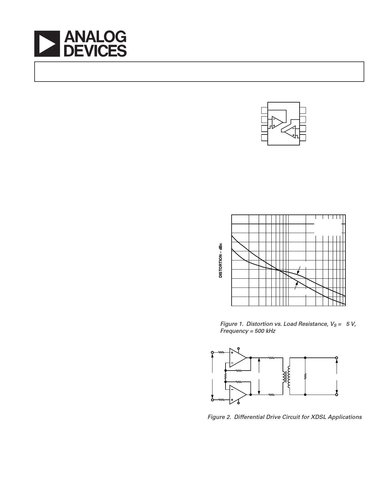
Figure 1. Distortion vs. Load Resistance, VS = ±5 V,
Frequency = 500 kHz
+VS
+
AMP 1
R1
+
VIN VREF
RL = 100⍀
OR
135⍀
LINE
VOUT POWER
IN dB
–
–VS
R2
Np:Ns
TRANSFORMER
–
Figure 2. Differential Drive Circuit for XDSL Applications
One Technology Way, P.O. Box 9106, Norwood, MA 02062-9106, U.S.A.
Tel: 781/329-4700
www.analog.com
Fax: 781/326-8703 © 2003 Analog Devices, Inc. All rights reserved.
1 page 
AD8012
MAXIMUM POWER DISSIPATION
The maximum power that can be safely dissipated by the AD8012
is limited by the associated rise in junction temperature. The maxi-
mum safe junction temperature for plastic encapsulated devices
is determined by the glass transition temperature of the plastic,
approximately +150°C. Temporarily exceeding this limit may
cause a shift in parametric performance due to a change in the
stresses exerted on the die by the package. Exceeding a junction
temperature of +175°C for an extended period can result in
device failure.
The output stage of the AD8012 is designed for maximum load
current capability. As a result, shorting the output to common
can cause the AD8012 to source or sink 500 mA. To ensure
proper operation, it is necessary to observe the maximum power
derating curves. Direct connection of the output to either power
supply rail can destroy the device.
Test Circuits
750⍀
750⍀
VOUT
RL
VIN
49.9⍀
0.1F
+
10F
+VS
0.1F
+
10F
–VS
Test Circuit 1. Gain = +2
2.0
1.5 8-LEAD SOIC
PACKAGE
1.0
TJ = 150؇C
0.5
8-LEAD
MSOP
0
–50 –40 –30 –20 –10 0 10 20 30 40 50 60 70 80 90
AMBIENT TEMPERATURE – ؇C
Figure 3. Plot of Maximum Power Dissipation vs.
Temperature for AD8012
750⍀
750⍀
VIN
53.6⍀
VOUT
RL
0.1F
0.1F
+
10F
+
10F
Test Circuit 2. Gain = –1
+VS
–VS
–4– REV. B
5 Page 
AD8012
9
8 ؎5V
7
6
5
+5V
4
3
2
1
0
10
100
LOAD – ⍀
1k
TPC 25. Output Swing vs. Load
10k
4.0
3.8
3.6
3.4
3.2
3.0
2.8
2.6
2.4
2.2
2.0
100
30
28
26
24
22
20
CURRENT NOISE
+IN/–IN
18
16
14
VOLTAGE NOISE
12
1k 10k
FREQUENCY – Hz
10
100k
TPC 26. Noise vs. Frequency
9
8
f = 5MHz
7 G = ؉2
RF = 750⍀
6
5
RL = 1k⍀
RL = 100⍀
4
3
2
1
0
3 4 5 6 7 8 9 10
TOTAL SUPPLY VOLTAGE ؊ V
TPC 27. Output Swing vs. Supply
11
G = +2
RF = 750⍀
RL = 100⍀
2V STEP
0.1%
5ns
t=0
TPC 28. Settling Time, VS = ±5 V
5
4
VO = 0.3V p-p
RF = 750⍀
3 RL = 1k⍀
2
1
0
G = +1
–1
G = +10
–2
G = +2
–3
–4
–5
1
10 100
FREQUENCY – MHz
500
TPC 29. Frequency Response; VS = ±5 V
0.5
0.4 VO = 0.3V p-p
G = +2
0.3 RF = 750⍀
RL = 1k⍀
0.2
0.1
0
–0.1
–0.2
–0.3
–0.4
–0.5
0.1
1 10
FREQUENCY – MHz
100
TPC 30. Gain Flatness; VS = ±5 V
–10–
REV. B
11 Page | ||
| Páginas | Total 17 Páginas | |
| PDF Descargar | [ Datasheet AD8012.PDF ] | |
Hoja de datos destacado
| Número de pieza | Descripción | Fabricantes |
| AD8010 | 200 mA Output Current High Speed Amplifier | Analog Devices |
| AD8011 | 300 MHz Current Feedback Amplifier | Analog Devices |
| AD8012 | Dual 350 MHz Low Power Amplifier | Analog Devices |
| AD8013 | Single Supply/ Low Power/ Triple Video Amplifier | Analog Devices |
| Número de pieza | Descripción | Fabricantes |
| SLA6805M | High Voltage 3 phase Motor Driver IC. |
Sanken |
| SDC1742 | 12- and 14-Bit Hybrid Synchro / Resolver-to-Digital Converters. |
Analog Devices |
|
DataSheet.es es una pagina web que funciona como un repositorio de manuales o hoja de datos de muchos de los productos más populares, |
| DataSheet.es | 2020 | Privacy Policy | Contacto | Buscar |