|
|
|
PDF 74ACTQ573 Data sheet ( Hoja de datos )
| Número de pieza | 74ACTQ573 | |
| Descripción | Quiet Series Octal Latch | |
| Fabricantes | Fairchild Semiconductor | |
| Logotipo | ||
Hay una vista previa y un enlace de descarga de 74ACTQ573 (archivo pdf) en la parte inferior de esta página. Total 12 Páginas | ||
|
No Preview Available !
January 1990
Revised October 2000
74ACQ573 • 74ACTQ573
Quiet Series Octal Latch with 3-STATE Outputs
General Description
The ACQ/ACTQ573 is a high-speed octal latch with buff-
ered common Latch Enable (LE) and buffered common
Output Enable (OE) inputs. The ACQ/ACTQ573 is func-
tionally identical to the ACQ/ACTQ373 but with inputs and
outputs on opposite sides of the package. The ACQ/ACTQ
utilizes Fairchild’s Quiet Series technology to guarantee
quiet output switching and improved dynamic threshold
performance. FACT Quiet Series features GTO output
control and undershoot corrector in addition to a split
ground bus for superior performance.
Features
s ICC and IOZ reduced by 50%
s Guaranteed simultaneous switching noise level and
dynamic threshold performance
s Guaranteed pin-to-pin skew AC performance
s Improved latch-up immunity
s Inputs and outputs on opposite sides of package allow
easy interface with microprocessors
s Outputs source/sink 24 mA
Ordering Code:
Order Number Package Number
Package Description
74ACQ573SC
M20B
20-Lead Small Outline Integrated Circuit (SOIC), JEDEC MS-013, 0.300 Wide
74ACQ573SJ
M20D
20-Lead Small Outline Package (SOP), EIAJ TYPE II, 5.3mm Wide
74ACQ573MTC
MTC20
20-Lead Thin Shrink Small Outline Package (TSSOP), JEDEC MO-153, 4.4mm Wide
74ACQ573PC
N20A
20-Lead Plastic Dual-In-Line Package (PDIP), JEDEC MS-001, 0.300 Wide
74ACTQ573SC
M20B
20-Lead Small Outline Integrated Circuit (SOIC), JEDEC MS-013, 0.300 Wide
74ACTQ573SJ
M20D
20-Lead Small Outline Package (SOP), EIAJ TYPE II, 5.3mm Wide
74ACTQ573QSC
MQA20
20-Lead Quarter Size Outline Package (QSOP), JEDEC MO-137, 0.150 Wide
74ACTQ573MTC
MTC20
20-Lead Thin Shrink Small Outline Package (TSSOP), JEDEC MO-153, 4.4mm Wide
74ACTQ573PC
N20A
20-Lead Plastic Dual-In-Line Package (PDIP), JEDEC MS-001, 0.300 Wide
Device also available in Tape and Reel. Specify by appending suffix letter “X” to the ordering code.
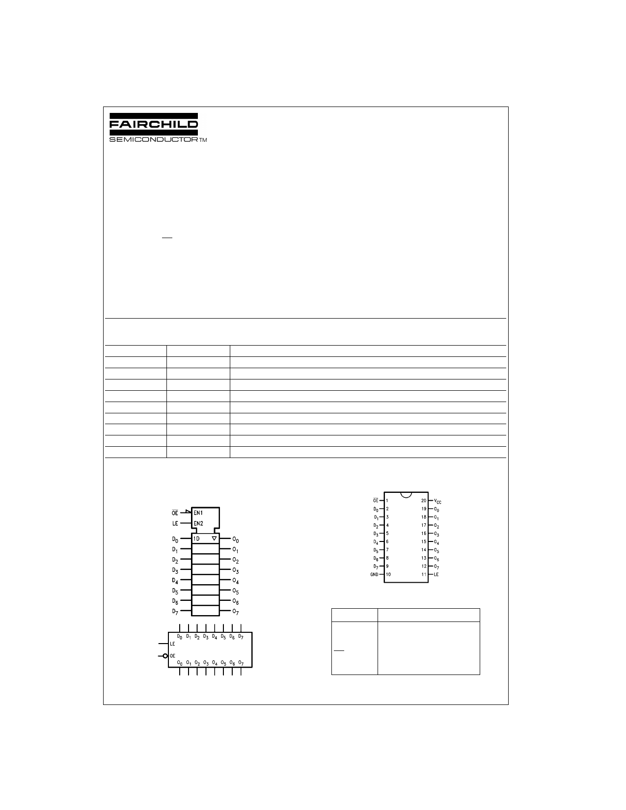
Logic Symbols
Connection Diagram
IEEE/IEC
Pin Descriptions
Pin Names
Description
D0–D7
LE
Data Inputs
Latch Enable Input
OE 3-STATE Output Enable Input
O0–O7
3-STATE Latch Outputs
FACT, Quiet Series, FACT Quiet Series, and GTO are trademarks of Fairchild Semiconductor Corporation
© 2000 Fairchild Semiconductor Corporation DS010633
www.fairchildsemi.com
1 page 
AC Electrical Characteristics for ACQ
VCC
TA = +25°C
TA = −40°C to +85°C
Symbol
Parameter
(V) CL = 50 pF
CL = 50 pF
Units
(Note 13)
Min
Typ
Max
Min
Max
tPHL Propagation Delay
tPLH
Dn to On
tPLH Propagation Delay
tPHL
LE to On
tPZL Output Enable Time
tPZH
tPHZ Output Disable Time
tPLZ
tOSHL
Output to Output Skew (Note 14)
tOSLH
Dn to On
Note 13: Voltage Range 5.0 is 5.0V ± 0.5V
3.3 2.5 8.5 10.5 2.5 11.0
5.0 1.5 5.5 7.0 1.5 7.5
3.3 2.5 8.5 12.0 2.5 12.5
5.0 2.0 6.0 8.0 2.0 8.5
3.3 2.5 8.5 13.0 2.5 13.5
5.0 1.5 6.0 8.5 1.5 9.0
3.3 1.0 9.0 14.5 1.0 15.0
5.0 1.0 6.0 9.5 1.0 10.0
3.3 1.0 1.5 1.5
5.0 0.5 1.0 1.0
ns
ns
ns
ns
ns
Voltage Range 3.3 is 3.3V ± 0.3V
Note 14: Skew is defined as the absolute value of the difference between the actual propagation delay for any two separate outputs of the same device. The
specification applies to any outputs switching in the same direction, either HIGH-to-LOW (tOSHL) or LOW-to-HIGH (tOSLH). Parameter guaranteed by design.
AC Operating Requirements for ACQ
Symbol
Parameter
tS Setup Time, HIGH or LOW
Dn to LE
tH Hold Time, HIGH or LOW
Dn to LE
tW LE Pulse Width, HIGH
Note 15: Voltage Range 5.0 is 5.0V ± 0.5V
Voltage Range 3.3 is 3.3V ± 0.3V
VCC
(V)
(Note 15)
3.3
5.0
3.3
5.0
3.3
5.0
TA = +25°C
TA = −40°C to +85°C
CL = 50 pF
CL = 50 pF
Typ Guaranteed Minimum
0 3.0
3.0
0 3.0
3.0
0 1.5
1.5
0 1.5
1.5
2.0 4.0
4.0
2.0 4.0
4.0
Units
ns
ns
ns
AC Electrical Characteristics for ACTQ
VCC
TA = +25°C
TA = −40°C to +85°C
Symbol
Parameter
(V) CL = 50 pF
CL = 50 pF
Units
(Note 16)
Min
Typ
Max
Min
Max
tPHL Propagation Delay
tPLH
Dnto On
tPLH Propagation Delay
tPHL
LE to On
tPZL, tPZH
Output Enable Time
tPHZ, tPLZ
Output Disable Time
tOSHL
Output to Output Skew (Note 17)
tOSLH
Dn to On
Note 16: Voltage Range 5.0 is 5.0V ± 0.5V
5.0 2.0 6.5 7.5 2.0 8.0 ns
5.0 2.5 7.0 8.5 2.5 9.0 ns
5.0 2.0 7.0 9.0 2.0 9.5 ns
5.0 1.0 8.0 10.0 1.0 10.5 ns
5.0 0.5 1.0 1.0 ns
Note 17: Skew is defined as the absolute value of the difference between the actual propagation delay for any two separate outputs of the same device. The
specification applies to any outputs switching in the same direction, either HIGH-to-LOW (tOSHL) or LOW-to-HIGH (tOSLH). Parameter guaranteed by design.
5 www.fairchildsemi.com
5 Page 
Physical Dimensions inches (millimeters) unless otherwise noted (Continued)
20-Lead Thin Shrink Small Outline Package (TSSOP), JEDEC MO-153, 4.4mm Wide
Package Number MTC20
11 www.fairchildsemi.com
11 Page | ||
| Páginas | Total 12 Páginas | |
| PDF Descargar | [ Datasheet 74ACTQ573.PDF ] | |
Hoja de datos destacado
| Número de pieza | Descripción | Fabricantes |
| 74ACTQ573 | Quiet Series Octal Latch | Fairchild Semiconductor |
| 74ACTQ574PC | Quiet Series Octal D-Type Flip-Flop with 3-STATE Outputs | Fairchild Semiconductor |
| 74ACTQ574SC | Quiet Series Octal D-Type Flip-Flop with 3-STATE Outputs | Fairchild Semiconductor |
| 74ACTQ574SJ | Quiet Series Octal D-Type Flip-Flop with 3-STATE Outputs | Fairchild Semiconductor |
| Número de pieza | Descripción | Fabricantes |
| SLA6805M | High Voltage 3 phase Motor Driver IC. |
Sanken |
| SDC1742 | 12- and 14-Bit Hybrid Synchro / Resolver-to-Digital Converters. |
Analog Devices |
|
DataSheet.es es una pagina web que funciona como un repositorio de manuales o hoja de datos de muchos de los productos más populares, |
| DataSheet.es | 2020 | Privacy Policy | Contacto | Buscar |