|
|
PDF N84C162 Data sheet ( Hoja de datos )
| Número de pieza | N84C162 | |
| Descripción | Supervisory Circuits | |
| Fabricantes | ON Semiconductor | |
| Logotipo | ||
Hay una vista previa y un enlace de descarga de N84C162 (archivo pdf) en la parte inferior de esta página. Total 11 Páginas | ||
|
No Preview Available !
N84C161, N84C162
Product Preview
Supervisory Circuits with
I2C Serial CMOS EEPROM,
Precision Reset Controller
and Watchdog Timer (16K)
www.onsemi.com
Description
The N84C161/2 is a complete memory and supervisory solution for
microcontroller−based systems. A serial EEPROM memory (16K)
with hardware memory write protection, a system power supervisor
with brown out protection and a watchdog timer are integrated
together in low power CMOS technology. Memory interface is via an
I2C bus.
SOIC−8
CASE 751BD
The 1.6−second watchdog circuit returns a system to a known good
state if a software or hardware glitch halts or “hangs” the system. The
N84C161 watchdog monitors the SDA line, making an additional PC
PIN CONFIGURATION
board trace unnecessary. The lower cost N84C162 does not have a
DC 1
8 VCC
watchdog timer.
The power supply monitor and reset circuit protects memory and
system controllers during power up/down and against brownout
conditions. Five reset threshold voltages support 5 V, 3.3 V and 3 V
RESET
WP
GND
2 N84C161 7
3 N84C162 6
45
RESET
SCL
SDA
systems. If power supply voltages are out of tolerance reset signals
become active, preventing the system microcontroller, ASIC or
peripherals from operating. Reset signals become inactive typically
PIN FUNCTIONS
200 ms after the supply voltage exceeds the reset threshold level. With
Pin Name Function
both active high and low reset signals, interface to microcontrollers
and other ICs is simple. In addition, a reset pin can be used as a
debounced input for pushbutton manual reset capability.
The N84C161/2 memory features a 16−byte page. In addition,
DC
RESET
WP
Do Not Connect
Active Low Reset I/O
Write Protect
hardware data protection is provided by a write protect pin WP and by
GND
Ground
a VCC sense circuit that prevents writes to memory whenever VCC falls
below the reset threshold or until VCC reaches the reset threshold
during power up.
These devices are available in a green SOIC−8 package.
Features
SDA
SCL
RESET
VCC
Serial Data/Address
Clock Input
Active High Reset I/O
Power Supply
• Watchdog Monitors SDA Signal (N84C161)
• 400 kHz I2C Bus Compatible
ORDERING INFORMATION
• 2.7 V to 6 V Operation
For Ordering Information details, see page 11.
• Low Power CMOS Technology
• 16−Byte Page Write Buffer
• Built−in Inadvertent Write Protection
♦ VCC Lock Out
♦ Write Protection Pin, WP
• 1,000,000 Program/Erase Cycles
• Manual Reset
• 100 Year Data Retention
• Active High or Low Reset
• 8−Pin SOIC
♦ Precision Power Supply Voltage Monitor
♦ 5 V, 3.3 V and 3 V Systems
♦ Five Threshold Voltage Options
• Commercial and Industrial Temperature Ranges
• These Devices are Pb−Free, Halogen Free/BFR Free
and are RoHS Compliant
This document contains information on a product under development. ON Semiconductor
reserves the right to change or discontinue this product without notice.
© Semiconductor Components Industries, LLC, 2016
September, 2016 − Rev. P0
1
Publication Order Number:
N84C161/D
1 page 
N84C161, N84C162
PIN DESCRIPTION
WP: WRITE PROTECT
If the pin is tied to VCC the entire memory array becomes
Write Protected (READ only). When the pin is tied to GND
or left floating normal read/write operations are allowed to
the device.
RESET/RESET: RESET I/O
These are open drain pins and can be used as reset trigger
inputs. By forcing a reset condition on the pins the device
will initiate and maintain a reset condition. The RESET pin
must be connected through a pulldown resistor, and the
RESET pin must be connected through a pull−up resistor.
SDA: SERIAL DATA ADDRESS
The bidirectional serial data/address pin is used to transfer
all data into and out of the device. The SDA pin is an open
drain output and can be wire−ORed with other open drain or
open collector outputs.
If there is no transition on the SDA for more than
1.6 seconds, the watchdog timer times out.
SCL: Serial Clock
Serial clock input.
DEVICE OPERATION
Reset Controller Description
The N84C161/2 precision RESET controller ensures
correct system operation during brownout and power
up/down conditions. It is configured with open drain
RESET outputs. During power−up, the RESET outputs
remain active until VCC reaches the VTH threshold and will
continue driving the outputs for approximately 200 ms
(tPURST) after reaching VTH. After the tPURST timeout
interval, the device will cease to drive the reset outputs. At
this point the reset outputs will be pulled up or down by their
respective pull up/down resistors. During power−down, the
RESET outputs will be active when VCC falls below VTH.
The RESET outputs will be valid so long as VCC is > 1.0 V
(VRVALID).
The RESET pins are I/Os; therefore, the N84C161/2 can
act as a signal conditioning circuit for an externally applied
manual reset. The inputs are edge triggered; that is, the
RESET input in the N84C161/2 will initiate a reset timeout
after detecting a low to high transition and the RESET input
will initiate a reset timeout after detecting a high to low
transition.
Watchdog Timer
The Watchdog Timer provides an independent protection
for microcontrollers. During a system failure, the N84C161
will respond with a reset signal after a time−out interval of
1.6 seconds for a lack of activity. The N84C161 is designed
with the Watchdog Timer feature on the SDA input. If the
microcontroller does not toggle the SDA input pin within 1.6
seconds, the Watchdog Timer times out. This will generate
a reset condition on reset outputs. The Watchdog Timer is
cleared by any transition on SDA.
As long as reset signal is asserted, the Watchdog Timer
will not count and will stay cleared.
The N84C162 does not have a Watchdog.
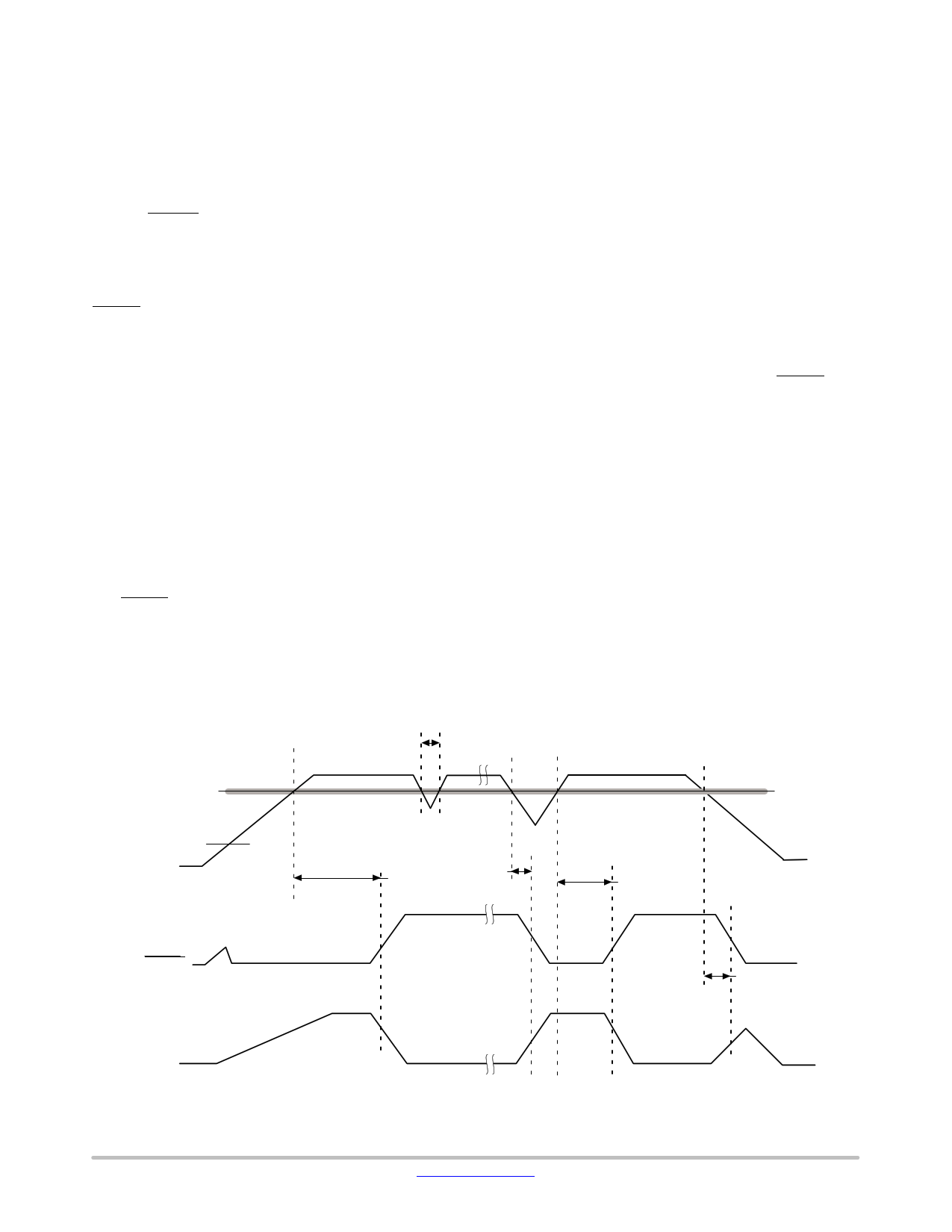
t
GLITCH
VTH
VRVA LI D
VCC
t PURS T
t RPD
t PURS T
RESET
t RPD
RESET
Figure 1. RESET Output Timing
www.onsemi.com
5
5 Page 
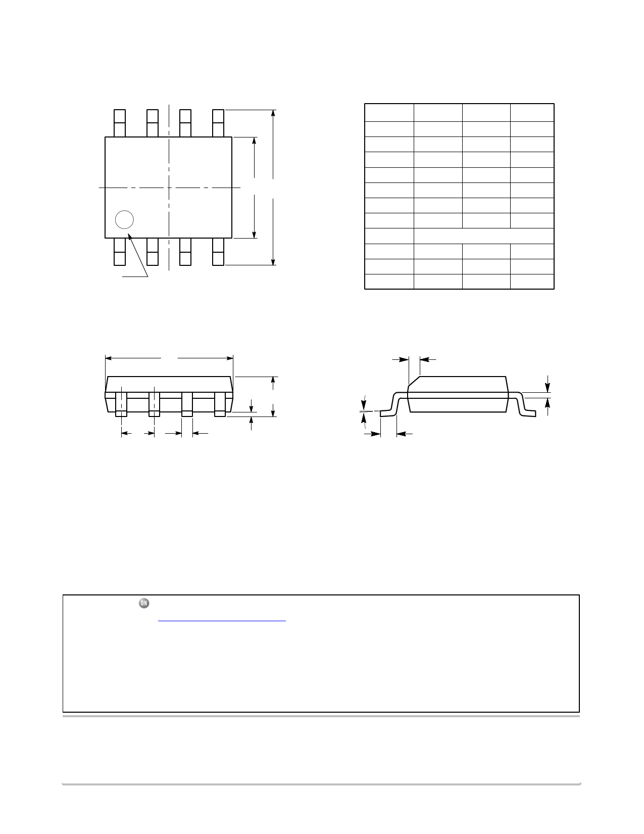
PIN # 1
IDENTIFICATION
TOP VIEW
N84C161, N84C162
SOIC 8, 150 mils
CASE 751BD−01
ISSUE O
E1 E
SYMBOL
A
A1
b
c
D
E
E1
e
h
L
θ
MIN
1.35
0.10
0.33
0.19
4.80
5.80
3.80
0.25
0.40
0º
NOM
1.27 BSC
MAX
1.75
0.25
0.51
0.25
5.00
6.20
4.00
0.50
1.27
8º
D
A1
A
eb
SIDE VIEW
Notes:
(1) All dimensions are in millimeters. Angles in degrees.
(2) Complies with JEDEC MS-012.
h
θ
L
END VIEW
c
ON Semiconductor is licensed by the Philips Corporation to utilize the I2C bus protocol.
ON Semiconductor and are trademarks of Semiconductor Components Industries, LLC dba ON Semiconductor or its subsidiaries in the United States and/or other countries.
ON Semiconductor owns the rights to a number of patents, trademarks, copyrights, trade secrets, and other intellectual property. A listing of ON Semiconductor’s product/patent
coverage may be accessed at www.onsemi.com/site/pdf/Patent−Marking.pdf. ON Semiconductor reserves the right to make changes without further notice to any products herein.
ON Semiconductor makes no warranty, representation or guarantee regarding the suitability of its products for any particular purpose, nor does ON Semiconductor assume any liability
arising out of the application or use of any product or circuit, and specifically disclaims any and all liability, including without limitation special, consequential or incidental damages.
Buyer is responsible for its products and applications using ON Semiconductor products, including compliance with all laws, regulations and safety requirements or standards,
regardless of any support or applications information provided by ON Semiconductor. “Typical” parameters which may be provided in ON Semiconductor data sheets and/or
specifications can and do vary in different applications and actual performance may vary over time. All operating parameters, including “Typicals” must be validated for each customer
application by customer’s technical experts. ON Semiconductor does not convey any license under its patent rights nor the rights of others. ON Semiconductor products are not
designed, intended, or authorized for use as a critical component in life support systems or any FDA Class 3 medical devices or medical devices with a same or similar classification
in a foreign jurisdiction or any devices intended for implantation in the human body. Should Buyer purchase or use ON Semiconductor products for any such unintended or unauthorized
application, Buyer shall indemnify and hold ON Semiconductor and its officers, employees, subsidiaries, affiliates, and distributors harmless against all claims, costs, damages, and
expenses, and reasonable attorney fees arising out of, directly or indirectly, any claim of personal injury or death associated with such unintended or unauthorized use, even if such
claim alleges that ON Semiconductor was negligent regarding the design or manufacture of the part. ON Semiconductor is an Equal Opportunity/Affirmative Action Employer. This
literature is subject to all applicable copyright laws and is not for resale in any manner.
PUBLICATION ORDERING INFORMATION
LITERATURE FULFILLMENT:
Literature Distribution Center for ON Semiconductor
19521 E. 32nd Pkwy, Aurora, Colorado 80011 USA
Phone: 303−675−2175 or 800−344−3860 Toll Free USA/Canada
Fax: 303−675−2176 or 800−344−3867 Toll Free USA/Canada
Email: [email protected]
N. American Technical Support: 800−282−9855 Toll Free
USA/Canada
Europe, Middle East and Africa Technical Support:
Phone: 421 33 790 2910
Japan Customer Focus Center
Phone: 81−3−5817−1050
ON Semiconductor Website: www.onsemi.com
Order Literature: http://www.onsemi.com/orderlit
For additional information, please contact your local
Sales Representative
◊
www.onsemi.com
N84C161/D
11
11 Page | ||
| Páginas | Total 11 Páginas | |
| PDF Descargar | [ Datasheet N84C162.PDF ] | |
Hoja de datos destacado
| Número de pieza | Descripción | Fabricantes |
| N84C161 | Supervisory Circuits | ON Semiconductor |
| N84C162 | Supervisory Circuits | ON Semiconductor |
| N84C163 | Supervisory Circuits | ON Semiconductor |
| Número de pieza | Descripción | Fabricantes |
| SLA6805M | High Voltage 3 phase Motor Driver IC. |
Sanken |
| SDC1742 | 12- and 14-Bit Hybrid Synchro / Resolver-to-Digital Converters. |
Analog Devices |
|
DataSheet.es es una pagina web que funciona como un repositorio de manuales o hoja de datos de muchos de los productos más populares, |
| DataSheet.es | 2020 | Privacy Policy | Contacto | Buscar |
