|
|
|
PDF 9FG430 Data sheet ( Hoja de datos )
| Número de pieza | 9FG430 | |
| Descripción | Four Output Differential Frequency Generator | |
| Fabricantes | IDT | |
| Logotipo | ||
Hay una vista previa y un enlace de descarga de 9FG430 (archivo pdf) en la parte inferior de esta página. Total 18 Páginas | ||
|
No Preview Available !
DATASHEET
Four Output Differential Frequency Generator
for PCIe Gen3 and QPI
9FG430
General Description:
The 9FG430 is a Frequency Timing Generator that provides 4
HCSL differential output pairs. These outputs support PCI-Express
Gen3, and QPI applications. The part supports Spread Spectrum
and synthesizes several additional output frequencies from either
a 14.31818 MHz crystal, a 25 MHz crystal or reference input clock.
The 9FG430 also outputs a copy of the reference clock. Complete
control of the device is available via strapping pins or via the
SMBus inteface.
Recommended Application:
4 Output Differential Frequency Generator for PCIe Gen3 and QPI
Output Features:
• 4 - 0.7V current mode differential HCSL output pairs
• 1 - 3.3V LVTTL REF output
Features/Benefits:
• Pin-to-Pin with 9FG104D/Easy upgrade to PCIe Gen3
• Generates common frequencies from 14.318 MHz or 25
MHz; single part supports mulitple applications
• Provides copy of reference output; eleminates need for
additional crystal or oscillator
• Unused outputs may be disabled in Hi-Z; save system
power
• Device may be configured by SMBus and/or strap pins;
can be used in systems without SMBus
Key Specifications:
• Cycle-to-cycle jitter: < 50ps with 25MHz input
• Output-to-output skew: <50ps
• Phase jitter: PCIe Gen3 < 1ps rms
• Phase jitter: QPI 9.6GB/s < 0.2ps rms
• 10 ppm synthesis error with 25MHz input and Spread Off
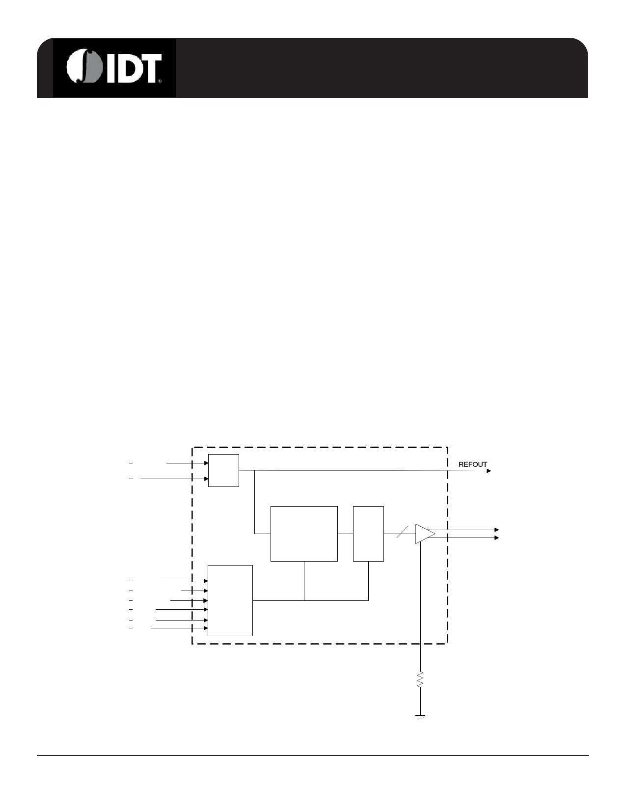
Functional Block Diagram
XIN/CLKIN
X2
OSC
REFOUT
PROGRAMMABLE
SPREAD PLL
STOP
LOGIC
4
DIF(3:0)
SPREAD
SEL14M_25M#
DIF_STOP#
FS(2:0)
SDATA
SCLK
CONTROL
LOGIC
IREF
IDT® Four Output Differential Frequency Generator for PCIe Gen3 and QPI
1
1681C—08/26/10
1 page 
9FG430
Four Output Differential Frequency Generator for PCIe Gen3 and QPI
Electrical Characteristics - DIF 0.7V Current Mode Differential Outputs
TA = TCOM or TIND; Supply Voltage VDD = 3.3 V +/-5%; See Test Loads s for loading conditions.
PARAMETER
SYMBOL
CONDITIONS
MIN TYP MAX UNITS NOTES
Slew rate
Trf
Scope averaging on
1
Slew rate matching ∆Trf Slew rate matching, Scope averaging on
4 V/ns 1, 2, 3
20 % 1, 2, 4
Voltage High
Voltage Low
VHigh
VLow
Statistical measurement on single-ended signal
using oscilloscope math function. (Scope
averaging on)
660
-150
850
mV
150
1
1
Max Voltage
Min Voltage
Vmax
Vmin
Measurement on single ended signal using
absolute value. (Scope averaging off)
-300
1150 mV
1
1
Vswing
Vswing
Scope averaging off
300
mV 1, 2
Crossing Voltage (abs) Vcross_abs
Scope averaging off
250 550 mV 1, 5
Crossing Voltage (var)
∆-Vcross
Scope averaging off
140 mV 1, 6
1Guaranteed by design and characterization, not 100% tested in production. IREF = VDD/(3xRR). For RR = 475Ω (1%), IREF = 2.32mA.
IOH = 6 x IREF and VOH = 0.7V @ ZO=50Ω (100Ω differential impedance).
2 Measured from differential waveform
3 Slew rate is measured through the Vswing voltage range centered around differential 0V. This results in a +/-150mV window around
differential 0V.
4 Matching applies to rising edge rate of Clock / falling edge rate of Clock#. It is measured in a +/-75mV window centered on the
average cross point where Clock rising meets Clock# falling. The median cross point is used to calculate the voltage thresholds the
oscilloscope uses for the edge rate calculations.
5 Vcross is defined as voltage where Clock = Clock# measured on a component test board and only applies to the differential rising
edge (i.e. Clock rising and Clock# falling).
6 The total variation of all Vcross measurements in any particular system. Note that this is a subset of V_cross_min/max (V_cross
absolute) allowed. The intent is to limit Vcross induced modulation by setting V_cross_delta to be smaller than V_cross absolute.
Electrical Characteristics - Current Consumption
TA = TCOM or TIND; Supply Voltage VDD = 3.3 V +/-5%, See Test Loads for loading
PARAMETER
SYMBOL
CONDITIONS
MIN
IDD3.3
VDD, All outputs active @100MHz
Operating Supply Current
IDDA3.3OP
IDD3.3
VDDA, All outputs active @100MHz
VDD, All outputs active @400MHz
IDDA3.3OP
VDDA, All outputs active @400MHz
IDD3.3PD
VDD, All differential pairs driven
Powerdown Current
IDDA3.3PD
IDD3.3PDZ
VDDA, All differential pairs driven
VDD, All differential pairs tri-stated
IDDA3.3PDZ
VDDA, All differential pairs tri-stated
1Guaranteed by design and characterization, not 100% tested in production.
2 IREF = VDD/(3xRR). For RR = 475Ω (1%), IREF = 2.32mA. IOH = 6 x IREF and VOH = 0.7V @ ZO=50Ω.
TYP
80
25
100
25
75
25
25
25
MAX
95
30
120
30
90
30
30
30
UNITS NOTES
mA 1
mA 1
mA 1
mA 1
mA 1
mA 1
mA 1
mA 1
Electrical Characteristics - Output Duty Cycle, Jitter, and Skew Characterisitics
TA = TCOM or TIND; Supply Voltage VDD = 3.3 V +/-5%, See Test Loads for loading
PARAMETER
SYMBOL
CONDITIONS
MIN
TYP
MAX UNITS NOTES
Duty Cycle
tDC Measured differentially, PLL Mode 45
55 % 1
Skew, Output to Output
tsk3
VT = 50%
50 ps 1
Jitter, Cycle to cycle
tjcyc-cyc
25M input
50 ps 1,3
Jitter, Cycle to cycle
tjcyc-cyc
14.318M input
60 ps 1,3
1Guaranteed by design and characterization, not 100% tested in production.
2 IREF = VDD/(3xRR). For RR = 475Ω (1%), IREF = 2.32mA. IOH = 6 x IREF and VOH = 0.7V @ ZO=50Ω.
3 Measured from differential waveform
4 Duty cycle distortion is the difference in duty cycle between the output and the input clock when the device is operated in bypass mode.
IDT® Four Output Differential Frequency Generator for PCIe Gen3 and QPI
5
1681C—08/26/10
5 Page 
9FG430
Four Output Differential Frequency Generator for PCIe Gen3 and QPI
General SMBus serial interface information for the 9FG430
How to Write:
• Controller (host) sends a start bit.
• Controller (host) sends the write address DC (H)
• IDT clock will acknowledge
• Controller (host) sends the begining byte location = N
• IDT clock will acknowledge
• Controller (host) sends the data byte count = X
• IDT clock will acknowledge
• Controller (host) starts sending Byte N through
Byte N + X -1
(see Note 2)
• IDT clock will acknowledge each byte one at a time
• Controller (host) sends a Stop bit
How to Read:
• Controller (host) will send start bit.
• Controller (host) sends the write address DC (H)
• IDT clock will acknowledge
• Controller (host) sends the begining byte
location = N
• IDT clock will acknowledge
• Controller (host) will send a separate start bit.
• Controller (host) sends the read address DD (H)
• IDT clock will acknowledge
• IDT clock will send the data byte count = X
• IDT clock sends Byte N + X -1
• IDT clock sends Byte 0 through byte X (if X(H)
was written to byte 8).
• Controller (host) will need to acknowledge each byte
• Controllor (host) will send a not acknowledge bit
• Controller (host) will send a stop bit
Index Block Write Operation
Controlle r (Host)
T starT bit
IDT (Sla ve /Re ce ive r)
S lave Address DC(H)
W R W Rite
ACK
Beginning Byte = N
ACK
Data Byte Count = X
ACK
Beginning Byte N
ACK
Byte N + X - 1
P stoP bit
ACK
Index Block Read Operation
Controlle r (Host)
IDT (Sla ve /Re ce ive r)
T starT bit
S lave Address DC(H)
W R W Rite
ACK
Beginning Byte = N
ACK
RT Repeat starT
S lave Address DD(H)
RD ReaD
ACK
ACK
ACK
Data Byte Count = X
Beginning Byte N
N Not acknowledge
P stoP bit
Byte N + X - 1
IDT® Four Output Differential Frequency Generator for PCIe Gen3 and QPI
11
1681C—08/26/10
11 Page | ||
| Páginas | Total 18 Páginas | |
| PDF Descargar | [ Datasheet 9FG430.PDF ] | |
Hoja de datos destacado
| Número de pieza | Descripción | Fabricantes |
| 9FG430 | Four Output Differential Frequency Generator | IDT |
| Número de pieza | Descripción | Fabricantes |
| SLA6805M | High Voltage 3 phase Motor Driver IC. |
Sanken |
| SDC1742 | 12- and 14-Bit Hybrid Synchro / Resolver-to-Digital Converters. |
Analog Devices |
|
DataSheet.es es una pagina web que funciona como un repositorio de manuales o hoja de datos de muchos de los productos más populares, |
| DataSheet.es | 2020 | Privacy Policy | Contacto | Buscar |