|
|
|
PDF DA14582 Data sheet ( Hoja de datos )
| Número de pieza | DA14582 | |
| Descripción | Low Power Bluetooth Smart SoC | |
| Fabricantes | Dialog Semiconductor | |
| Logotipo | ||
Hay una vista previa y un enlace de descarga de DA14582 (archivo pdf) en la parte inferior de esta página. Total 30 Páginas | ||
|
No Preview Available !
DATASHEET - PRELIMINARY
MARCH 11, 2015 V2.0
DA14582
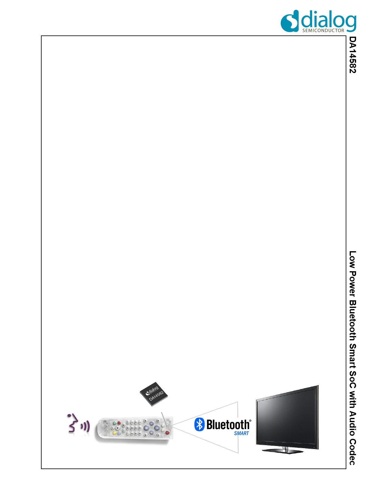
Low Power Bluetooth Smart SoC with Audio Codec
General description
16 MHz 32 bit ARM Cortex-M0 with SWD I/F
The DA14582 integrated circuit has a fully integrated
radio transceiver, baseband processor for Bluetooth®
Smart with Audio Codec.
Dedicated Link Layer Processor
AES-128 bit encryption Processor
Memories
32 kB One-Time-Programmable (OTP) memory
The DA14582 is optimized for remote control units
42 kB System SRAM
(RCU) requiring support for voice commands and
84 kB ROM
motion/gesture recognition. Its integrated analog wide
8 kB Retention SRAM
band audio codec provides native support for analog
Power management
microphones thereby reducing the total number of
Integrated Buck DC-DC converter
components of the system while its optimized package
P0, P1, P2 and P3 ports with 3.3 V tolerance
enables designs using single-layer FR1 PCBs further-
Easy decoupling of only 4 supply pins
more contributing to the reduction of the cost of the
Supports coin (typ. 3.0 V) and alkaline (typ. 1.5 V)
system.
battery cells
The DA14582 supports a flexible memory architecture
for storing Bluetooth profiles and custom application
code, which can be updated over the air (OTA). The
qualified Bluetooth Smart protocol stack is stored in a
dedicated ROM. All software runs on the ARM® Cor-
tex®-M0 processor via a simple scheduler.
10-bit ADC for battery voltage measurement
Digital controlled oscillators
16 MHz crystal (±20 ppm max) and RC oscillator
32 kHz crystal (±50 ppm, ±500 ppm max) and
RCX oscillator
General purpose, Capture and Sleep timers
Digital interfaces
The Bluetooth Smart firmware includes the L2CAP ser-
29 General purpose I/Os
vice layer protocols, Security Manager (SM), Attribute
2 UARTs with hardware flow control up to 1 MBd
Protocol (ATT), the Generic Attribute Profile (GATT)
SPI+™ interface
and the Generic Access Profile (GAP). All profiles pub-
I2C bus at 100 kHz, 400 kHz
lished by the Bluetooth SIG as well as custom profiles
3-axis capable Quadrature Decoder
are supported.
Analog interfaces
The transceiver interfaces directly to the antenna and
is fully compliant with the Bluetooth 4.1 standard.
4-channel 10-bit ADC
14 bits wide band Codec with microphone and
28 loudspeaker analog front-end
The DA14582 has dedicated hardware for the Link
Layer implementation of Bluetooth®Smart and inter-
Radio transceiver
Fully integrated 2.4 GHz CMOS transceiver
face controllers for enhanced connectivity capabilities.
Single wire antenna: no RF matching or RX/TX
switching required
Features
Supply current at VBAT3V:
Complies with Bluetooth V4.1, ETSI EN 300 328 and
EN 300 440 Class 2 (Europe), FCC CFR47 Part 15
(US) and ARIB STD-T66 (Japan)
Processing power
TX: 3.4 mA, RX: 3.7 mA (with ideal DC-DC)
0 dBm transmit output power
-20 dBm output power in “Near Field Mode”
-93 dBm receiver sensitivity
________________________________________________________________________________________________
System diagram
© 2015 Dialog Semiconductor
1 www.dialog-semiconductor.com
1 page 
Table 2: Pin Description
PIN NAME
TYPE
General Purpose I/Os
P0_0
P0_1
P0_2
P0_3/
P0_4/SPI_DI
P0_5/16MCLK
P0_6
P0_7
DIO
DIO
DIO
DIO
DIO
DIO
DIO
DIO
P1_0
P1_1
P1_2
P1_3
P1_4/SWCLK
P1_5/SW_DIO
DIO
DIO
DIO
DIO
DIO
DIO
P2_0
P2_1/SPI_EN
P2_2
P2_3
P2_4
P2_5
P2_6
P2_7
P2_8
P2_9
DIO
DIO
DIO
DIO
DIO
DIO
DIO
DIO
DIO
DIO
P3_0
P3_1 (Table 3)
P3_2 (Table 3)
P3_3
P3_5
P3_6
P3_7
DIO
DIO
DIO
DIO
DIO
DIO
DIO
Debug interface
SW_DIO/P1_5
DIO
Drive
(mA)
4.8
4.8
4.8
4.8
4.8
SW_CLK/P1_4
Clocks
XTAL16Mp
XTAL16Mm
XTAL32kp
XTAL32km
DIO
AI
AO
AI
AO
4.8
Reset
state
(Note )
DESCRIPTION
I-PD
I-PD
I-PD
I-PD
I-PD
I-PD
I-PD
I-PD
I-PD
I-PD
I-PD
I-PD
I-PD
I-PU
I-PD
I-PD
I-PD
I-PD
I-PD
I-PD
I-PD
I-PD
I-PD
I-PD
I-PD
I-PD
I-PD
I-PD
I-PD
I-PD
I-PD
INPUT/OUTPUT with selectable pull up/down resistor. Pull-
down enabled during and after reset. General purpose I/O port
bit or alternate function nodes. Contains state retention mecha-
nism during power down.
INPUT/OUTPUT with selectable pull up/down resistor. Pull-
down enabled during and after reset. General purpose I/O port
bit or alternate function nodes. Contains state retention mecha-
nism during power down.
This signal is the JTAG clock by default
This signal is the JTAG data I/O by default
INPUT/OUTPUT with selectable pull up/down resistor. Pull-
down enabled during and after reset. General purpose I/O port
bit or alternate function nodes. Contains state retention mecha-
nism during power down.
INPUT/OUTPUT with selectable pull up/down resistor. Pull-
down enabled during and after reset. General purpose I/O port
bit or alternate function nodes. Contains state retention mecha-
nism during power down.
I-PU
I-PD
INPUT/OUTPUT. JTAG Data input/output. Bidirectional data and
control communication. Can also be used as a GPIO
INPUT JTAG clock signal. Can also be used as a GPIO
INPUT. Crystal input for the 16 MHz XTAL
OUTPUT. Crystal output for the 16 MHz XTAL
INPUT. Crystal input for the 32.768 kHz XTAL
OUTPUT. Crystal output for the 32.768 kHz XTAL
© 2015 Dialog Semiconductor
4 Preliminary - March 11, 2015 v2.0
5 Page 
• Programming of the Bluetooth device address
• Programming of the trimming value for the external
16 MHz crystal.
This mode of operation applies to the final product and
is performed by the customer. During this phase, cer-
tain fields in the OTP should be programmed
3.5 POWER MODES
There are four different power modes in the DA14582:
• Active mode: System is active and operates at full
speed.
• Sleep mode: No power gating has been pro-
grammed, the ARM CPU is idle, waiting for an inter-
rupt. PD_SYS is on. PD_PER and PED_RAD
depending on the programmed enabled value.
• Extended Sleep mode: All power domains are off
except for the PD_AON, the programmed PD_RRx
and the PD_SR. Since the SysRAM retains its data,
no OTP mirroring is required upon waking up the
system.
• Deep Sleep mode: All power domains are off except
for the PD_AON and the programmed PD_RRx.
This mode dissipates the minimum leakage power.
However, since the SysRAM has not retained its
data, an OTP mirror action is required upon waking
up the system.
3.6 INTERFACES
3.6.1 UARTs
The UART is compliant to the industry-standard 16550
and is used for serial communication with a peripheral,
modem (data carrier equipment, DCE) or data set.
Data is written from a master (CPU) over the APB bus
to the UART and it is converted to serial form and
transmitted to the destination device. Serial data is also
received by the UART and stored for the master (CPU)
to read back.
There is no DMA support on the UART block since its
contains internal FIFOs. Both UARTs support hard-
ware flow control signals (RTS, CTS, DTR, DSR).
Features
• 16 bytes Transmit and receive FIFOs
• Hardware flow control support (CTS/RTS)
• Shadow registers to reduce software overhead and
also include a software programmable reset
• Transmitter Holding Register Empty (THRE) inter-
rupt mode
• IrDA 1.0 SIR mode supporting low power mode.
• Functionality based on the 16550 industry standard:
• Programmable character properties, such as num-
ber of data bits per character (5-8), optional
• parity bit (with odd or even select) and number of
stop bits (1, 1.5 or 2)
• Line break generation and detection
• Prioritized interrupt identification
• Programmable serial data baud rate as calculated
by the following: baud rate = (serial clock frequency)/
(divisor).
3.6.2 SPI+
This interface supports a subset of the Serial Periph-
eral Interface SPITM. The serial interface can transmit
and receive 8, 16 or 32 bits in master/slave mode and
transmit 9 bits in master mode. The SPI + interface has
enhanced functionality with bidirectional 2x16-bit word
FIFOs.
SPI™ is a trademark of Motorola, Inc.
Features
• Slave and Master mode
• 8 bit, 9 bit, 16 bit or 32 bit operation
• Clock speeds upto 16 MHz for the SPI controller.
Programmable output frequencies of SPI source
clock divided by 1, 2, 4, 8
• SPI clock line speed up to 8 MHz
• SPI mode 0, 1, 2, 3 support (clock edge and phase)
• Programmable SPI_DO idle level
• Maskable Interrupt generation
• Bus load reduction by unidirectional writes-only and
reads-only modes.
Built-in RX/TX FIFOs for continuous SPI bursts.
3.6.3 I2C interface
The I2C interface is a programmable control bus that
provides support for the communications link between
Integrated Circuits in a system. It is a simple two-wire
bus with a software-defined protocol for system control,
which is used in temperature sensors and voltage level
translators to EEPROMs, general-purpose I/O, A/D
and D/A converters.
Features
• Two-wire I2C serial interface consists of a serial data
line (SDA) and a serial clock (SCL)
• Two speeds are supported:
• Standard mode (0 to 100 kbit/s)
• Fast mode (<= 400 kbit/s)
• Clock synchronization
• 32 deep transmit/receive FIFOs
• Master transmit, Master receive operation
• 7 or 10-bit addressing
© 2015 Dialog Semiconductor
10 Preliminary - March 11, 2015 v2.0
11 Page | ||
| Páginas | Total 30 Páginas | |
| PDF Descargar | [ Datasheet DA14582.PDF ] | |
Hoja de datos destacado
| Número de pieza | Descripción | Fabricantes |
| DA14580 | Low Power Bluetooth Smart SoC | Dialog Semiconductor |
| DA14581 | Low Power Bluetooth Smart SoC | Dialog Semiconductor |
| DA14582 | Low Power Bluetooth Smart SoC | Dialog Semiconductor |
| DA14583 | Low Power Bluetooth Smart SoC | Dialog Semiconductor |
| Número de pieza | Descripción | Fabricantes |
| SLA6805M | High Voltage 3 phase Motor Driver IC. |
Sanken |
| SDC1742 | 12- and 14-Bit Hybrid Synchro / Resolver-to-Digital Converters. |
Analog Devices |
|
DataSheet.es es una pagina web que funciona como un repositorio de manuales o hoja de datos de muchos de los productos más populares, |
| DataSheet.es | 2020 | Privacy Policy | Contacto | Buscar |