|
|
|
PDF EDI88512C Data sheet ( Hoja de datos )
| Número de pieza | EDI88512C | |
| Descripción | 512Kx8 Monolithic SRAM | |
| Fabricantes | Microsemi | |
| Logotipo | ||
Hay una vista previa y un enlace de descarga de EDI88512C (archivo pdf) en la parte inferior de esta página. Total 8 Páginas | ||
|
No Preview Available !
EDI88512C
512Kx8 Monolithic SRAM, CMOS
FEATURES
512Kx8 bit CMOS Static
Random Access Memory
• Access Times of 70, 85, 100ns
• Data Retention Function (LP version)
• TTL Compatible Inputs and Outputs
• Fully Static, No Clocks
32 lead JEDEC Approved Evolutionary Pinout
• Ceramic Sidebrazed 600 mil DIP (Package 9)
• Ceramic SOJ (Package 140)
Single +5V (±10%) Supply Operation
The EDI88512C is a 4 megabit Monolithic CMOS Static RAM.
The 32 pin DIP pinout adheres to the JEDEC evolutionary standard
for the four megabit device. Both the DIP and CSOJ packages
are pin for pin upgrades for the single chip enable 128K x 8, the
EDI88128C. Pins 1 and 30 become the higher order addresses.
A Low Power version with Data Retention (EDI88512LP) is also
available for battery backed applications. Military product is
available compliant to Appendix A of MIL-PRF-38535.
* This product is subject to change without notice.
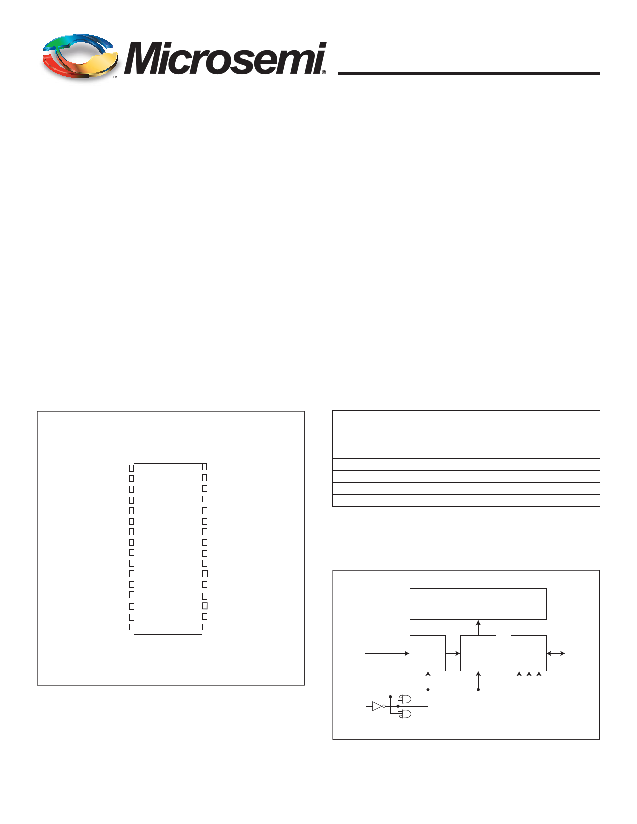
FIGURE 1 – PIN CONFIGURATION
32 PIN
TOP VIEW
A18 1
A16 2
A14 3
A12 4
A7 5
A6 6
A5 7
A4 8
A3 9
A2 10
A1 11
A0 12
I/O0 13
I/O1 14
I/O2 15
Vss 16
32 pin
Evolutionary
32 Vcc
31 A15
30 A17
29 WE#
28 A13
27 A8
26 A9
25 A11
24 OE#
23 A10
22 CS#
21 I/O7
20 I/O6
19 I/O5
18 I/O4
17 I/O3
I/O0-7
A0-18
WE#
CS#
OE#
VCC
VSS
NC
PIN DESCRIPTION
Data Inputs/Outputs
Address Inputs
Write Enables
Chip Selects
Output Enable
Power (+5V ±10%)
Ground
Not Connected
A0-18
WE#
CS#
OE#
BLOCK DIAGRAM
Memory Array
Address
Buffer
Address
Decoder
I/O
Circuits
I/O0-7
Microsemi Corporation reserves the right to change products or specifications without notice.
May 2014 © 2014 Microsemi Corporation. All rights reserved.
Rev. 13
1
Microsemi Corporation • (602) 437-1520 • www.microsemi.com/pmgp
1 page 
EDI88512C
Characteristic
Low Power Version only
Data Retention Voltage
Data Retention Quiescent Current
Chip Disable to Data Retention Time
Operation Recovery Time
DATA RETENTION CHARACTERISTICS (EDI88512LP ONLY)
-55°C ≤ TA ≤ +125°C
Sym Conditions Min Typ
VCC
ICCDR
tCDR
TR
VCC = 2.0V
CS# ≥ VCC -0.2V
VIN ≥ VCC -0.2V
or VIN ≤ 0.2V
2
–
0
tAVAV
–
–
–
–
Max
–
185
–
–
Units
V
μA
ns
ns
FIGURE 5 – DATA RETENTION – CS# CONTROLLED
DATA RETENTION MODE
VCC
4.5V 4.5V
VCC
tCDR
tR
CS# CS# = VCC -0.2V
DATA RETENTION, CS# CONTROLLED
Microsemi Corporation reserves the right to change products or specifications without notice.
May 2014 © 2014 Microsemi Corporation. All rights reserved.
Rev. 13
5
Microsemi Corporation • (602) 437-1520 • www.microsemi.com/pmgp
5 Page | ||
| Páginas | Total 8 Páginas | |
| PDF Descargar | [ Datasheet EDI88512C.PDF ] | |
Hoja de datos destacado
| Número de pieza | Descripción | Fabricantes |
| EDI88512C | 512Kx8 Monolithic SRAM | Microsemi |
| EDI88512CA | 512Kx8 Monolithic SRAM/ SMD 5962-95600 | ETC |
| EDI88512CA | 512Kx8 Monolithic SRAM | Microsemi |
| EDI88512CA-XMXG | 512Kx8 Plastic Monolithic SRAM CMOS | Microsemi |
| Número de pieza | Descripción | Fabricantes |
| SLA6805M | High Voltage 3 phase Motor Driver IC. |
Sanken |
| SDC1742 | 12- and 14-Bit Hybrid Synchro / Resolver-to-Digital Converters. |
Analog Devices |
|
DataSheet.es es una pagina web que funciona como un repositorio de manuales o hoja de datos de muchos de los productos más populares, |
| DataSheet.es | 2020 | Privacy Policy | Contacto | Buscar |