|
|
|
PDF ST6265B Data sheet ( Hoja de datos )
| Número de pieza | ST6265B | |
| Descripción | 8-bit MCUs | |
| Fabricantes | STMicroelectronics | |
| Logotipo | ||
Hay una vista previa y un enlace de descarga de ST6265B (archivo pdf) en la parte inferior de esta página. Total 30 Páginas | ||
|
No Preview Available !
ST6255C ST6265C
ST6265B
8-bit MCUs with ADC,
safe reset, auto-reload timer, EEPROM and SPI
Features
■ 3.0 to 6.0V supply operating range
■ 8 MHz maximum clock frequency
■ -40 to +125°C operating temperature range
■ Run, Wait and Stop modes
■ 5 interrupt vectors
■ Look-up table capability in program memory
■ Data storage in program memory:
user selectable size
■ Data RAM: 128 bytes
■ Data EEPROM: 128 bytes (not in ST6255C)
■ User programmable options
■ 21 I/O pins, fully programmable as:
– Input with pull-up resistor
– Input without pull-up resistor
– Input with interrupt generation
– Open-drain or push-pull output
– Analog Input
■ 8 I/O lines can sink up to 30 mA to drive LEDs or
TRIACs directly
– 8-bit Timer/Counter with 7-bit programmable
prescaler
■ 8-bit Auto-reload timer with 7-bit programmable
prescaler (AR Timer)
■ Digital watchdog
■ Oscillator safe guard (not in ST6265B ROM
devices)
■ Low voltage detector for safe reset (not in
ST6265B ROM devices)
■ 8-bit A/D converter with 13 analog inputs
■ 8-bit synchronous peripheral interface (SPI)
■ On-chip clock oscillator can be driven by quartz
crystal, ceramic resonator or RC network
■ User configurable power-on reset
■ One external non-maskable interrupt
■ ST626x-EMU2 Emulation and Development
System (connects to an MS-DOS PC via a
parallel port)
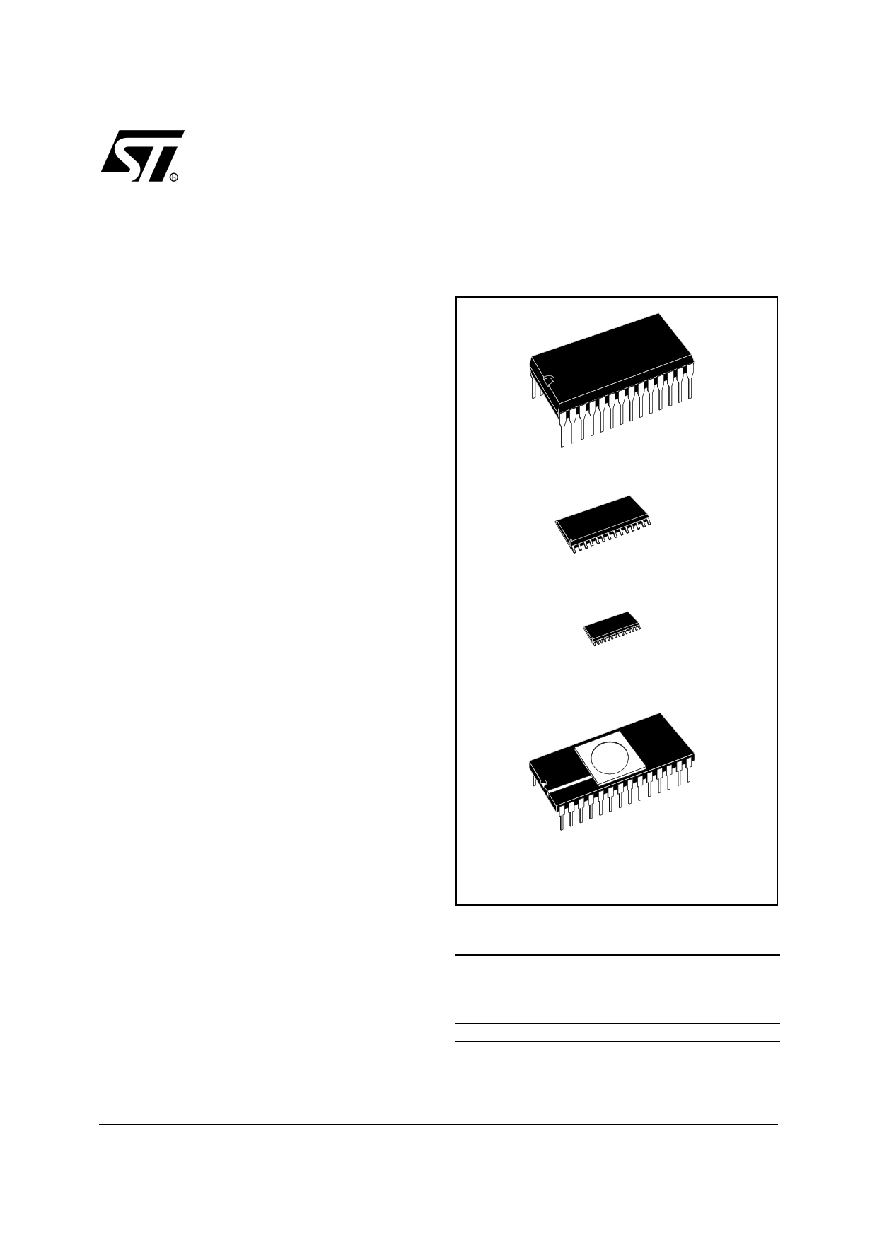
PDIP28
PS028
SS0P28
CDIP28W
(See end of Datasheet for Ordering Information)
Table 1. Device summary
Partnumber
ST6255C
ST6265C
ST6265B
OTP/EPROM/ROM
program memory
(Bytes)
3884
3884
3884
EEPROM
(Bytes)
-
128
128
March 2009
Rev 3
1/84
1 page 
ST6255C ST6265C ST6265B
1.3 MEMORY MAP
1.3.1 Introduction
The MCU operates in three separate memory
spaces: Program space, Data space, and Stack
space. Operation in these three memory spaces is
described in the following paragraphs.
Figure 3. Memory Addressing Diagram
Briefly, Program space contains user program
code in OTP and user vectors; Data space con-
tains user data in RAM and in OTP, and Stack
space accommodates six levels of stack for sub-
routine and interrupt service routine nesting.
0000h
PROGRAM SPACE
PROGRAM
MEMORY
0-63
0FF0h
0FFFh
INTERRUPT &
RESET VECTORS
DATA SPACE
000h
RAM / EEPROM
BANKING AREA
03Fh
040h
07Fh
080h
081h
082h
083h
084h
DATA READ-ONLY
MEMORY WINDOW
X REGISTER
Y REGISTER
V REGISTER
W REGISTER
RAM
0C0h
0FFh
DATA READ-ONLY
MEMORY
WINDOW SELECT
DATA RAM
BANK SELECT
ACCUMULATOR
5/84
5 Page 
ST6255C ST6265C ST6265B
MEMORY MAP (Cont’d)
Additional Notes on Parallel Mode:
If the user wishes to perform parallel program-
ming, the first step should be to set the E2PAR2
bit. From this time on, the EEPROM will be ad-
dressed in write mode, the ROW address and the
data will be latched and it will be possible to
change them only at the end of the programming
cycle or by resetting E2PAR2 without program-
ming the EEPROM. After the ROW address is
latched, the MCU can only “see” the selected
EEPROM row and any attempt to write or read
other rows will produce errors.
The EEPROM should not be read while E2PAR2
is set.
As soon as the E2PAR2 bit is set, the 8 volatile
ROW latches are cleared. From this moment on,
the user can load data in all or in part of the ROW.
Setting E2PAR1 will modify the EEPROM regis-
ters corresponding to the ROW latches accessed
after E2PAR2. For example, if the software sets
E2PAR2 and accesses the EEPROM by writing to
addresses 18h, 1Ah and 1Bh, and then sets
E2PAR1, these three registers will be modified si-
multaneously; the remaining bytes in the row will
be unaffected.
Note that E2PAR2 is internally reset at the end of
the programming cycle. This implies that the user
must set the E2PAR2 bit between two parallel pro-
gramming cycles. Note that if the user tries to set
E2PAR1 while E2PAR2 is not set, there will be no
programming cycle and the E2PAR1 bit will be un-
affected. Consequently, the E2PAR1 bit cannot be
set if E2ENA is low. The E2PAR1 bit can be set by
the user, only if the E2ENA and E2PAR2 bits are
also set.
Notes: The EEPROM page shall not be changed
through the DRBR register when the E2PAR2 bit
is set.
EEPROM Control Register (EECTL)
Address: EAh — Read/Write
Reset status: 00h
7
D7
E2O
FF
D5
0
D4
E2PA E2PA E2BU E2E
R1 R2 SY NA
Bit 7 = D7: Unused.
Bit 6 = E2OFF: Stand-by Enable Bit. WRITE ONLY.
If this bit is set the EEPROM is disabled (any access
will be meaningless) and the power consumption of
the EEPROM is reduced to its lowest value.
Bit 5-4 = D5-D4: Reserved. MUST be kept reset.
Bit 3 = E2PAR1: Parallel Start Bit. WRITE ONLY.
Once in Parallel Mode, as soon as the user software
sets the E2PAR1 bit, parallel writing of the 8 adja-
cent registers will start. This bit is internally reset at
the end of the programming procedure. Note that
less than 8 bytes can be written if required, the un-
defined bytes being unaffected by the parallel pro-
gramming cycle; this is explained in greater detail in
the Additional Notes on Parallel Mode overleaf.
Bit 2 = E2PAR2: Parallel Mode En. Bit. WRITE
ONLY. This bit must be set by the user program in
order to perform parallel programming. If E2PAR2
is set and the parallel start bit (E2PAR1) is reset,
up to 8 adjacent bytes can be written simultane-
ously. These 8 adjacent bytes are considered as a
row, whose address lines A7, A6, A5, A4, A3 are
fixed while A2, A1 and A0 are the changing bits, as
illustrated in Figure 4. E2PAR2 is automatically re-
set at the end of any parallel programming proce-
dure. It can be reset by the user software before
starting the programming procedure, thus leaving
the EEPROM registers unchanged.
Bit 1 = E2BUSY: EEPROM Busy Bit. READ ON-
LY. This bit is automatically set by the EEPROM
control logic when the EEPROM is in program-
ming mode. The user program should test it before
any EEPROM read or write operation; any attempt
to access the EEPROM while the busy bit is set
will be aborted and the writing procedure in
progress will be completed.
Bit 0 = E2ENA: EEPROM Enable Bit. WRITE ON-
LY. This bit enables programming of the EEPROM
cells. It must be set before any write to the EEP-
ROM register. Any attempt to write to the EEP-
11/84
11 Page | ||
| Páginas | Total 30 Páginas | |
| PDF Descargar | [ Datasheet ST6265B.PDF ] | |
Hoja de datos destacado
| Número de pieza | Descripción | Fabricantes |
| ST6265B | 8-bit MCUs | STMicroelectronics |
| ST6265C | 8-bit MCUs | STMicroelectronics |
| Número de pieza | Descripción | Fabricantes |
| SLA6805M | High Voltage 3 phase Motor Driver IC. |
Sanken |
| SDC1742 | 12- and 14-Bit Hybrid Synchro / Resolver-to-Digital Converters. |
Analog Devices |
|
DataSheet.es es una pagina web que funciona como un repositorio de manuales o hoja de datos de muchos de los productos más populares, |
| DataSheet.es | 2020 | Privacy Policy | Contacto | Buscar |